








Schedule a Call Back


3 Manufacturing Challenges Created by Vertically Stacked Dies
 Articles
- Oct 01,26
Vertically stacked dies boost chip performance but create major challenges in heat management, interconnect testing and nanometre-scale inspection, writes Emily Newton.

Traditional methods of packing more transistors onto silicon chips have reached their physical limits. Vertically stacked dies solve this problem by building upward instead of outward, delivering massive performance improvements. However, 3D integration introduces three critical manufacturing hurdles. The industry must manage extreme heat density, verify microscopic vertical interconnects and inspect buried layers with nanometer precision before this technology can reach its full potential.
1. The Thermal Management Crisis
Stacking multiple dies vertically shortens interconnect lengths, which can boost performance. However, the trade-off is severe thermal management issues that traditional 2D designs never had to contend with.
Integrating multiple dies vertically dramatically increases power density. Each additional layer compounds the problem because heat generation scales faster than the available pathways for dissipation can accommodate. Advanced 3D integrated circuit (IC) packaging designs concentrate power dissipation in smaller volumes and create intricate thermal routes that make heat management more challenging. Cooling strategies that worked reliably for planar architectures become inadequate when power sources stack on top of each other.
Vertical thermal resistance becomes the limiting factor. Inner dies embedded deep within a 3D stack have almost no direct access to cooling solutions. Heat must travel through multiple layers of silicon and interconnect materials before reaching a heat sink. This creates hot spots that can exceed safe operating temperatures and degrade device reliability over time. Architecting and building thermal interfaces between each die adds substantial complexity to an already demanding manufacturing process.
2. Forming and Testing Microscopic Vertical Interconnects
Through-Silicon Vias (TSVs) and microbumps enable 3D structures by drilling through thinned silicon wafers and creating electrical pathways between stacked dies. Testing these connections for defects without destroying the fragile substrates requires fundamentally new approaches.
Modern semiconductor devices operate as complete systems-on-a-chip that integrate all necessary components into a unified package. A single failed interconnect in a vertically stacked die can render the entire expensive unit useless. Manufacturers must verify the integrity of thousands of microscopic connections during both pre-bond and post-bond assembly phases. The stakes increase even more when dealing with high-value memory and logic combinations where even one design defect can waste months of production effort.
Working with ultra-thin wafers gets more complicated. Because substrates are reduced to thinner layers, standard probing techniques can crack or damage them. Non-contact electrical testing methods and optical inspection technologies have emerged to address this problem, though this adds cost and complexity to an already expensive manufacturing process.
3. Metrology Techniques for Vertically Stacked Dies
Confirming the alignment and integrity of buried layers and vertical connections in vertically stacked dies is one of the semiconductor industry's most pressing metrology challenges. Traditional 2D measurement techniques lack the penetration depth and precision needed for accurate analysis of internal structures.
3D chip architecture demands solutions for greater quality control at every stage of the manufacturing process, down to the nanometer scale. Defects buried between layers can go unchecked until final testing, when the cost of failure peaks and production timelines run short.
A single undetected misalignment can force manufacturers to scrap an entire multi-die stack that has already undergone weeks of costly processing. X-ray imaging and acoustic microscopy can provide some visibility into hidden structures, but these methods have limitations in detail and throughput.
Achieving the extreme accuracy and stability needed to inspect these intricate 3D architectures depends on the hardware required for these new, complex inspection tools. Precision motion control stages enable nanometer-scale positioning repeatability across large substrates. Without this level of control, manufacturers cannot reliably detect alignment errors and structural defects that would compromise device performance.
Why the Performance Payoff Outweighs the Hurdles
Vertically stacked dies deliver gains that traditional scaling approaches can no longer achieve. Bandwidth increases dramatically when memory sits on top of processing logic because data travels over micrometers rather than centimeters. Latency can also drop substantially compared to conventional package designs.
Compact devices in industrial automation and mobile applications benefit from the footprint reduction this architecture provides. Data centers see lower operating costs and reduced thermal loads, thanks to better power efficiency. Research confirms that some heterogeneous 3D-stacked ICs can achieve up to a 23% improvement in performance per cost and a 16% improvement in power delay when compared to traditional 2D counterparts.
These gains translate to faster processing speeds for real-time control systems and lower energy consumption in high-performance computing environments, where every watt saved reduces cooling infrastructure requirements and operational expenses. Such advantages make 3D integration essential for next-generation semiconductor products. The manufacturing headaches become worthwhile investments later, when the end result enables capabilities that would otherwise remain impossible.
Overcoming Physical Production Hurdles for Future Innovation
The future of semiconductor innovation depends on solving fundamental physical production problems. Thermal management, interconnect integrity and metrology for buried layers will determine which companies successfully commercialize 3D integration. Industrial automation and advanced manufacturing sectors now await the maturation of these solutions before the full promise of vertically stacked dies can transform operations.
About the author:
Emily Newton is a tech and industrial journalist and the Editor-in-Chief of Revolutionized magazine. Subscribe to the Revolutionized newsletter for more content from Emily.
Image Courtesy: Magnific.com
Vertically Stacked Dies
3D Integration
Thermal Management
Through-Silicon Vias
Semiconductor Metrology
Microbumps
Precision Motion Control
Advanced Packaging
Related Stories
Smart Manufacturing
3 Manufacturing Challenges Created by Vertically Stacked Dies
Vertically stacked dies boost chip performance but create major challenges in heat management, interconnect testing and nanometre-scale inspection, writes Emily Newton.
Read moreElectrical & Electronics

ATS India partners with Hirata to advance semiconductor automation in India
ATS India and Hirata Corporation have partnered to bring advanced semiconductor automation and material-handling technologies to India, supporting the growth of domestic manufacturing capabilities.
Read moreAutomation & Robotics
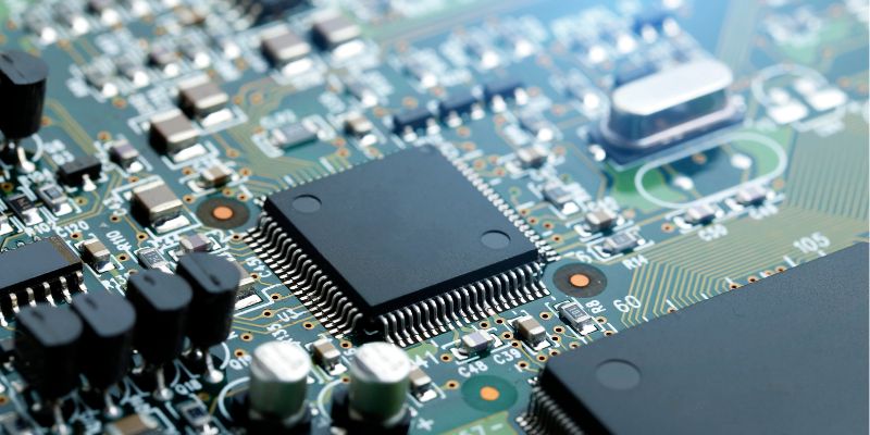
Global Chip Equipment Sales Set to Reach US$229.5 Billion by 2028
SEMI forecasts global semiconductor equipment sales at US$165.9 billion in 2026, driven by AI, advanced memory, packaging and expanding chipmaking capacity.
Read moreRelated Products
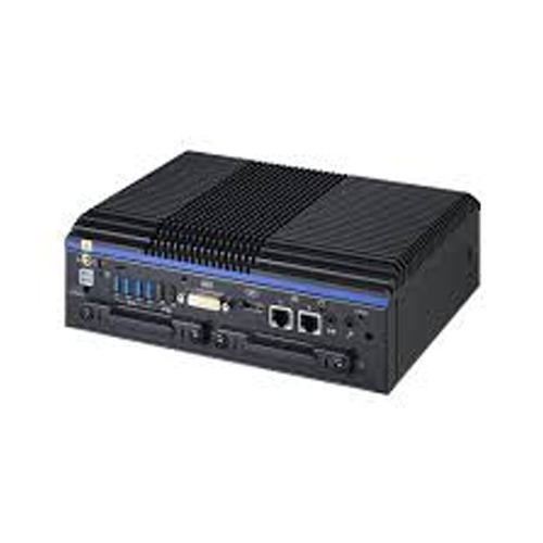
Fanless Industrial Pc for Smart Manufacturing
Smart Manufacturing
CONTEC Launches BX-M4600 Series - Fanless Industrial PC for Smart Manufacturing.
latest News
Subscribe to iNoW

For Industry News on WhatsApp, Give a Miss Call on: +91 84228 74016